






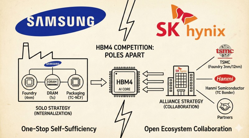
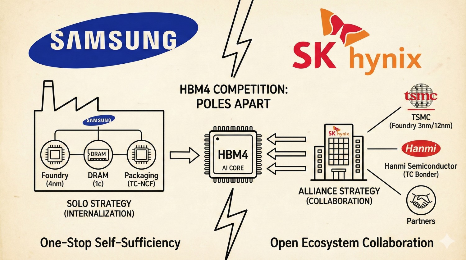
From base die to back-end processes, Samsung Electronics plans to secure technological superiority through an internalization strategy encompassing foundry and equipment. In contrast, SK Hynix is leveraging an open collaboration model that mobilizes the entire external ecosystem including TSMC and Hanmi Semiconductor, leading with verified quality and speed.
HBM plays the role of quickly delivering necessary data to GPUs responsible for AI computations within a certain time. No matter how fast the GPU calculates, bottlenecks occur if data is not delivered on time. HBM is a structure that innovatively increases data processing speed by vertically stacking multiple DRAM chips.
Individual DRAM chips that make up HBM are called 'core dies.' The chip located at the bottom layer is specifically designated as the 'base die (logic die).' The base die performs the critical role of directly connecting to the GPU, interpreting signals, and delivering commands to upper core dies.
Until HBM3E (5th generation), memory companies produced base dies using their own DRAM processes, but from HBM4 (6th generation), foundry (contract manufacturing) methods utilizing cutting-edge fine processes are being introduced to improve speed and power efficiency.
SK Hynix is entrusting HBM4 base die production to Taiwan's TSMC. This is because the company judged that process optimization collaboration with TSMC is essential to meet performance requirements demanded by customers. SK Hynix is known to plan to utilize TSMC's 3-nanometer (nm) and 12nm processes. Standard products for servers will be manufactured with 12nm, while customized products such as Nvidia premium GPUs and Google's custom chips (TPU) are expected to be produced with 3nm processes.
In contrast, Samsung Electronics produces HBM4 base dies using its own foundry 4nm process. Although negotiations with customers over price and volume are variables, if Samsung Electronics secures prices similar to SK Hynix, it can create a relatively higher profit structure through internalization.
Samsung Electronics, a latecomer in HBM, has a strategy of securing customers by leveraging technological capabilities. Samsung Electronics applies the 1c (6th generation) process to HBM4 DRAM.
관련기사
Samsung Electronics and SK Hynix Eye KRW 150 Trillion Operating Profit EraSamsung Electronics’ Jun Young-hyun Bets on HBM4 — Decision Expected in Q1 Next YearSamsung Foundry Seeks Rebound with ‘Made in America’ DriveSK Hynix Surges to 41% Operating Margin in Q2; Puts Full Force Behind HBM4 Pricing Defense
This is choosing a process one generation ahead of SK Hynix, which maintains the 1b (5th generation) process applied to existing HBM3E for HBM4 as well.
The HBM4 performance disclosed by the two companies in October also shows differences.
Samsung Electronics specifically presented data transfer (I/O) speed and bandwidth at maximum 11Gbps and 2.8TB per second, respectively. SK Hynix only disclosed minimum levels as 'above 10Gbps' and 'above 2.6TB.' This means that even the minimum standards meet Nvidia's enhanced performance requirements.
An industry official said, "For Samsung Electronics, securing yield is key," adding, "As a leading HBM company, SK Hynix's intention to prioritize stable supply is evident."
Packaging (back-end process) strategies also differ significantly between the two companies. The core back-end process in HBM is a type of bonding process that connects stacked DRAMs. From HBM4 20-stack and above, hybrid bonding is required for yield stabilization, but previous generations are likely to maintain existing technologies.
SK Hynix uses the 'MR-MUF process' that fills the space between chips with liquid protective material after soldering. The TC (thermal compression) bonder equipment that temporarily fixes chips to substrates and chips to chips just before this process is supplied by Hanmi Semiconductor, Hanwha Semitech, and others. Since even slight misalignment causes defects, TC bonders for HBM4 are known as expensive equipment costing approximately KRW 4 billion per unit.
If SK Hynix can be likened to 'applying wood glue,' Samsung Electronics can be compared to 'attaching double-sided tape.' This is the 'TC-NCF' method that inserts film-type protective material between layers and proceeds with thermal compression. Samsung Electronics mainly receives TC bonder supplies from its subsidiary SEMES.
Gwak Horyung (horr@fntimes.com)











![[THE COMPASS] 한미사이언스 경영권 분쟁, 신동국이 주도하는 ‘종식’ 게임](https://cfnimage.commutil.kr/phpwas/restmb_setimgmake.php?pp=006&w=69&h=45&m=5&simg=20261008122108000710a837df649412411124362.jpg&nmt=18)

![영업익 53% 뛴다는데…대웅제약 몸값 누르는 두 가지 변수 [5대 제약사 3Q 실적 ④]](https://cfnimage.commutil.kr/phpwas/restmb_setimgmake.php?pp=006&w=69&h=45&m=5&simg=202610081106100618007fd637f543112168227135.jpg&nmt=18)

![[기고] 앞으로 10년 뒤, 당신의 예금 통장은 과연 안전할까](https://cfnimage.commutil.kr/phpwas/restmb_setimgmake.php?pp=006&w=69&h=45&m=5&simg=20261008135710064190c1c16452b012411124362.jpg&nmt=18)


![[그래픽 뉴스] ‘순대’가 경제용어라고? 순(純)대외자산, 한국의 진짜 해외자산은 얼마일까?](https://cfnimage.commutil.kr/phpwas/restmb_setimgmake.php?pp=006&w=298&h=298&m=1&simg=202609021356075202de68fcbb3512411124362_0.jpg&nmt=18)
![[그래픽 뉴스] ISA 대개편! 나에게 유리한 계좌는?](https://cfnimage.commutil.kr/phpwas/restmb_setimgmake.php?pp=006&w=298&h=298&m=1&simg=202608041713155615de68fcbb3512411124362_0.jpg&nmt=18)
![[그래픽 뉴스] 미국 증시 새로운 키워드 'MANGOS'](https://cfnimage.commutil.kr/phpwas/restmb_setimgmake.php?pp=006&w=298&h=298&m=1&simg=202607291740382069de68fcbb3512411124362_0.jpg&nmt=18)

![[그래픽 뉴스] 은퇴후 30년 부모님 세대의 생존전략](https://cfnimage.commutil.kr/phpwas/restmb_setimgmake.php?pp=006&w=298&h=298&m=1&simg=202606301704439153de68fcbb3512411124362_0.jpg&nmt=18)
![[신간]은퇴연옥…김경록의 은퇴 후 삶의 나침반](https://cfnimage.commutil.kr/phpwas/restmb_setimgmake.php?pp=006&w=81&h=123&m=5&simg=20260414140833047280f8caa4a5ce12411124362.jpg&nmt=18)
![[신간] 물처럼 흐르고 원칙으로 서다…김용환의 통찰을 담다](https://cfnimage.commutil.kr/phpwas/restmb_setimgmake.php?pp=006&w=81&h=123&m=5&simg=20260409114249027860f8caa4a5ce12411124362.jpg&nmt=18)
![[안현정 서평] 플랫폼의 영지에서 ‘미학적 주권’을 선포하라...'K가 죽어야 K가 산다' 장준환 著](https://cfnimage.commutil.kr/phpwas/restmb_setimgmake.php?pp=006&w=81&h=123&m=5&simg=20260527121426063220c1c16452b012411124362.jpg&nmt=18)
![[서평] 추세 매매의 대가들...추세추종 투자전략의 대가 14인 인터뷰](https://cfnimage.commutil.kr/phpwas/restmb_setimgmake.php?pp=006&w=81&h=123&m=5&simg=2023102410444004986c1c16452b0175114235199.jpg&nmt=18)


![[머니무브 2026] “지금 사도 될까?” 답이 안 보인다면…하반기 투자, 4명의 전문가에게 물어보세요](https://cfnimage.commutil.kr/phpwas/restmb_setimgmake.php?pp=006&w=89&h=45&m=1&simg=202609151044050355302a735e27af12411124362.jpg&nmt=18)
![[AD] ‘PBV 라인업 확장’ 기아, 9월 독일서 ‘PV7’ 첫 공개](https://cfnimage.commutil.kr/phpwas/restmb_setimgmake.php?pp=006&w=89&h=45&m=1&simg=2026083111010602815074925877361231180222.jpg&nmt=18)
![[AD] 제네시스, 럭셔리 경험 더한 ‘2027 GV70’‧‘GV70 그래파이트’ 출시](https://cfnimage.commutil.kr/phpwas/restmb_setimgmake.php?pp=006&w=89&h=45&m=1&simg=20260702143546085600749258773622211122717.jpg&nmt=18)